Por el momento, esta página no está disponible en español. Puede obtener una traducción automática mediante la opción de traducción de Google.
No podemos responsabilizarnos de este servicio puesto que podemos no verificar los resultados de la traducción.
Si desea más información, póngase en contacto con nosotros.
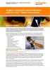
Semiconductors
Modern electronics use a wide range of semiconductor materials. Cutting edge devices, such as transistors, solar cells and light emitting diodes, push materials properties to their limits, and require extremely homogeneous source materials. Raman spectroscopy is an ideal tool for studying semiconductors.
Characterise semiconductors
You can use Raman to characterise and generate images of all semiconductors (e.g. Si, carbon-based, III-V's, and polymers) and superconductors. A wide range of information can be revealed, including:
- chemical composition (e.g. alloy fractions of compound semiconductors)
- polytypes (e.g. 4H-SiC and 6H-SicC)
- strain/stress
- dopant concentrations
- thin film thickness
- crystal structure type and orientation
- crystal quality
- uniformity and purity
- device temperature

Easy analysis
Raman analysis is simple because it requires no sample preparation. It does not require vacuum technology, or suffer from charging effects experienced with electron microscopy.
Renishaw can configure your Raman system to suit all users, from research scientists to technicians.
Large area analysis
Renishaw Raman systems can analyse very large samples. For example, you can generate images of entire wafers to discover contaminants or residual stresses.
PL characterisation
Renishaw's Raman systems also enable you to collect and analyse photoluminescence (PL) spectra. You can collect both vibrational and electronic information with one instrument.
Online systems
Add Renishaw's Raman systems to your production line to conduct online analysis for quality control purposes. Diagnose problems early, reduce waste and improve yield.
Reliable results
Renishaw's Raman systems produce highly repeatable data that accurately represents the sample. In-built automated calibration and health checking ensure data can be accurately compared, no matter when collected.
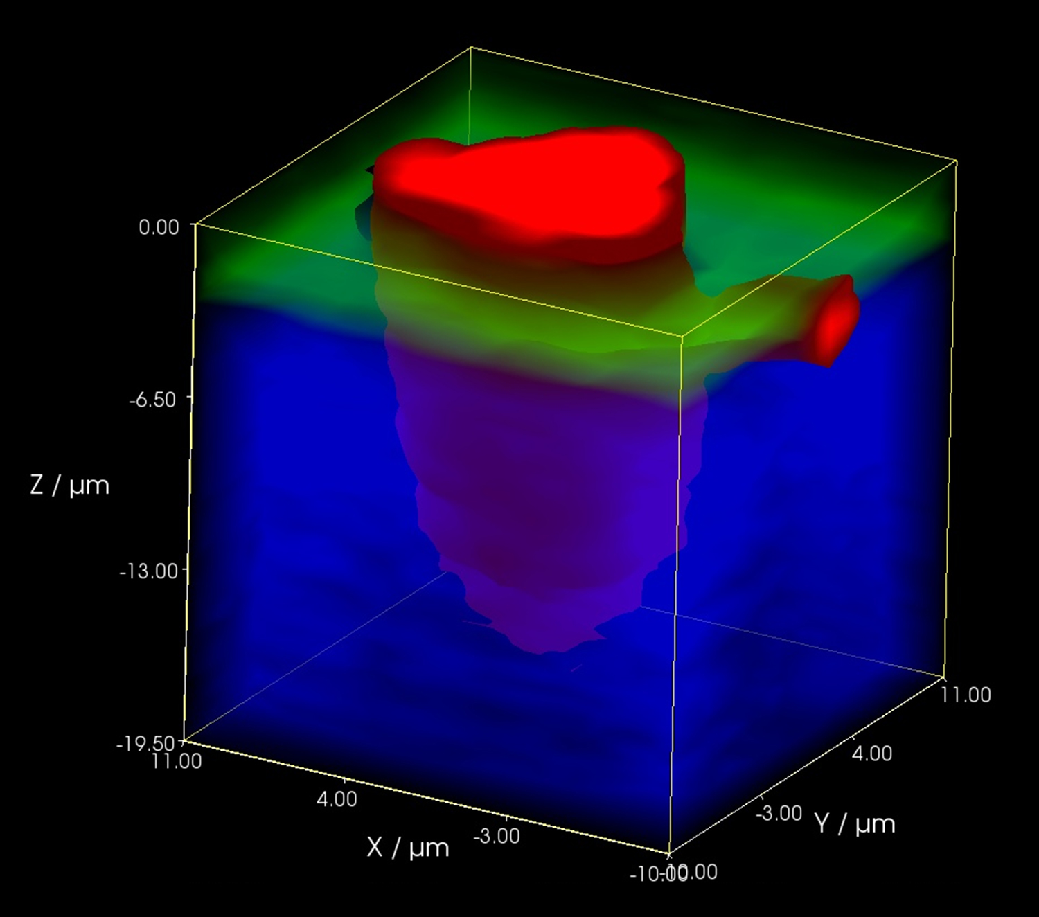
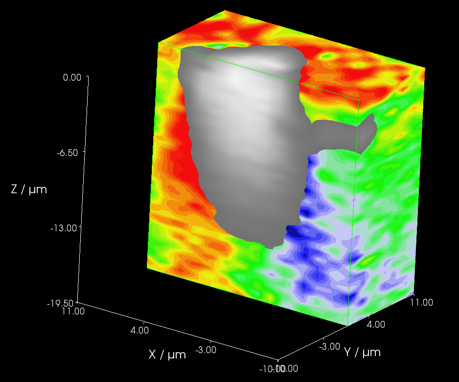
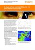
3D Raman map of a Silicon Carbide wafer

We're here when you need us
To find out more about this application area, or an application that isn't covered here, contact our applications team.
Contact our applications team
Downloads: materials science (semiconductors)
-
 Application note: Photocurrent measurements on the inVia™ confocal Raman microscope
When light interacts with semiconducting materials it can induce electrical currents (‘photocurrents’). These currents carry information about the electronic, optical, and charge transport properties of the material. This information is complementary to that obtainable from Raman scattering, which can identify physical changes in the material properties. This application note demonstrates the capability to simultaneously collect Raman and photocurrent data using the photocurrent mapping module concurrently with an inVia Raman microscope.
-
 Application note: Analyse compound semiconductors with the inVia™ Raman microscope
Over the last decade compound semiconductors have attracted a great deal of attention because they offer properties suitable for next generation devices in a wide range of application areas. Historically, the fabrication of these devices has been hindered by material challenges. While these have mainly been conquered at the research level, problems still persist when scaling up to industrial production. Renishaw’s inVia Raman microscope is a non-invasive, non-destructive characterisation tool which provides sub-micrometre information on the vibrational, crystal and electronic structure of materials.
-
 Application note: Analyse silicon carbide (SiC) with the inVia Raman microscope
The properties of silicon carbide are highly dependent on its crystal structure (it can exist in many polytypes), on the quality of the crystal, and on the number and types of defects present. Manufacturers of silicon carbide raw material and devices need to monitor and control these attributes to enhance yield. The first step in controlling these parameters is to measure them repeatably and quantifiably. Renishaw’s Raman systems are ideal for this.
-
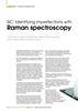
 News release: Identifying imperfections with Raman spectroscopy
An article in Compound Semiconductor magazine, October 2015, describes how Raman spectroscopy allows routine mapping of SiC wafers in little more than an hour.
Related stories
Caltech working to solve the world's energy problems with the help of inVia
The California Institute of Technology (Caltech) is on a mission to find new and effective ways to produce solar fuels using only sunlight, water and carbon dioxide. A focus of this is investigating photocatalysis and light capture.
Renishaw's inVia wins CS Industry Award 2016
Renishaw, the global engineering technologies company, is delighted to announce that it has received a CS Industry Award 2016, in the Metrology category, for its inVia Raman microscope. The CS Industry Awards are organised by Compound Semiconductor magazine and voted for through the website www.compoundsemiconductor.net Together these deliver comprehensive coverage of the compound semiconductor industry.